Double Sided Copper Clad PCB Board — Bare Copper on Both Sides, Ready to Etch
When your prototype layout demands copper on both sides and a clean, ready-to-etch surface, sourcing the right substrate can derail an entire build. Makers, electronics hobbyists, and small-batch PCB fabricators who need a dependable double-sided copper-clad sheet will find this board ready to mask, etch, and drill without the guesswork of inconsistent raw stock.
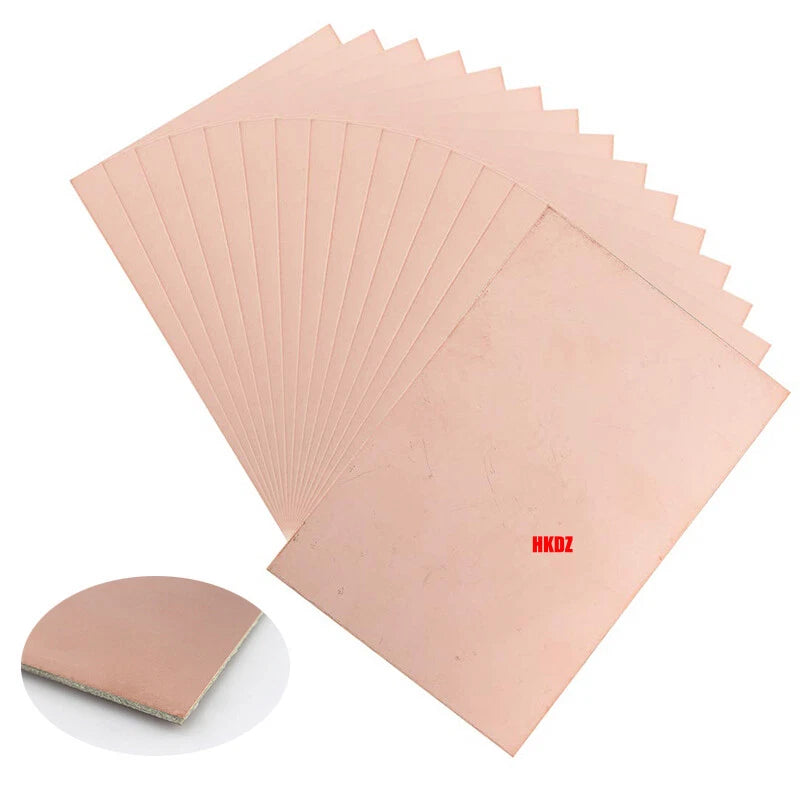
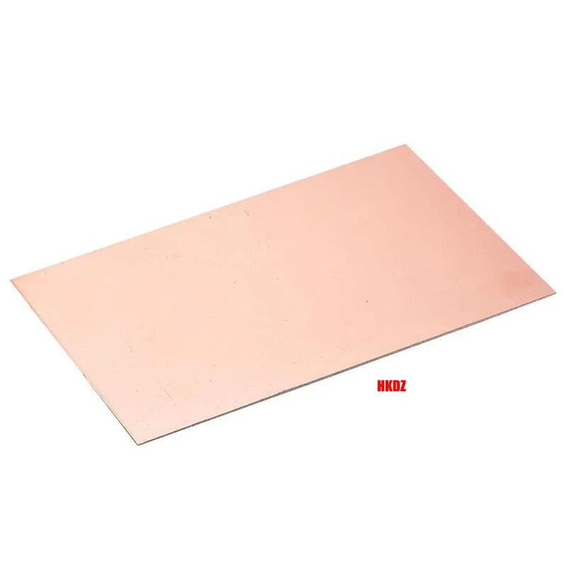
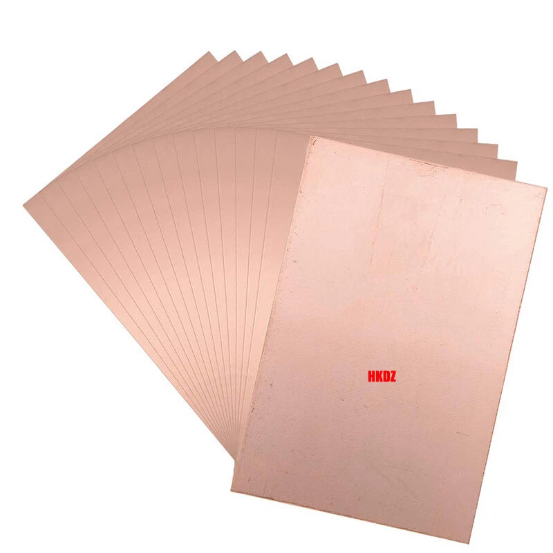
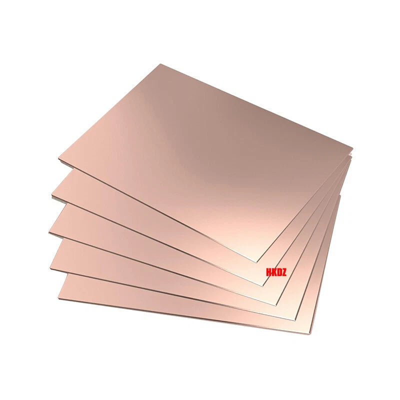
Each piece is a double-sided copper clad laminate with bare, bright copper foil bonded to both faces of an insulating core (plastic/phenolic resin substrate). No UV or photo-sensitive coating is applied — the copper surfaces are clean and uncoated straight out of the pack. Boards are available in eight cut sizes ranging from 5×7 cm (approx. 2"×2.75") up to 20×30 cm (approx. 7.9"×11.8"), and can be ordered in quantities from 1 to 50 pieces per variant. Substrate thickness is 1.5 mm.
Typical use cases include DIY PCB fabrication using toner-transfer or direct resist-pen methods, rapid prototyping of analog or digital circuits for maker workshops, and educational electronics projects where students practice circuit layout and etching on a double-sided copper-clad board.
⚠️ Warm Tips: There may be marks or scratches on the surface of the circuit board, but it will not affect its performance.
⚡ Compatible with ferric chloride / sodium persulfate etchants, toner-transfer film, resist pens, and dry-film photoresist laminate. Suitable for single-layer and double-layer through-hole and SMD prototype layouts.
Key Features
- 🔲 Double-Sided Bare Copper Cladding — Bright copper foil bonded to both faces of the insulating core, enabling two-layer circuit routing without additional lamination steps.
- 🪙 No UV or Photo-Sensitive Coating — Both copper faces are clean and uncoated, giving you full flexibility to apply your preferred resist method: toner transfer, resist pen, or dry-film laminate.
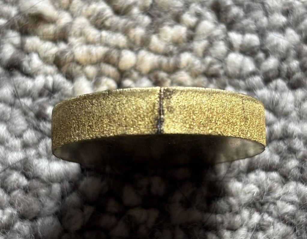
- 🧱 Insulating Core Visible at Edges — The plastic/phenolic substrate core is clearly visible at the shear-cut edges, confirming genuine double-sided construction with copper on both outer faces.
- 📐 Eight Cut Sizes Available — From compact 5×7 cm (2"×2.75") up to full-sheet 20×30 cm (7.9"×11.8"), covering small sensor boards to larger power-supply layouts.
- 📦 Flexible Quantity Options — Order 1 to 50 pieces per size, making it practical for one-off prototypes or small classroom and workshop batches.
- 🔩 Drillable Substrate — The 1.5 mm thick substrate supports standard PCB carbide drill bits (typically 0.8–3.2 mm) for through-hole component mounting and via creation.
Who Is This For
🔧 DIY Electronics Makers — Prototype your own PCB designs using toner transfer or resist-pen methods on a clean bare-copper surface.
🎓 Students & Educators — Ideal for classroom labs teaching circuit layout, etching chemistry, and hands-on PCB fabrication techniques.
💼 Small-Batch Fabricators — Order multi-packs to produce consistent prototype runs without the cost of professional PCB manufacturing.
⌚ Hobbyist Tinkerers — Perfect for Arduino shields, sensor breakouts, and custom control boards where off-the-shelf PCBs don't fit your exact layout.
Technical Specifications
| Board Type |
Double-Sided Copper Clad Laminate |
| Surface Treatment |
Bare copper — no UV or photo-sensitive coating |
| Copper Color |
Copper Tone (natural bare copper) |
| Substrate / Core Material |
Plastic / phenolic resin insulating core |
| Substrate Thickness |
1.5 mm |
| Available Sizes (cm) |
5×7, 7×10, 8×12, 10×10, 10×15, 12×18, 15×20, 20×30 |
| Available Sizes (inches, approx.) |
2"×2.75" up to 7.9"×11.8" |
| Quantity per Order |
1 / 2 / 3 / 5 / 8 / 10 / 15 / 20 / 25 / 30 / 40 / 50 PCS |
| Edge Finish |
Guillotine shear-cut |
| Product Type |
Copper Sheet / PCB Substrate |
Frequently Asked Questions
Which size should I choose for a standard Arduino shield layout?
An Arduino Uno shield footprint is approximately 68×53 mm. The 7×10 cm (70×100 mm) or 8×12 cm (80×120 mm) boards both provide enough clearance for the shield outline plus a small border for handling. If you need extra routing space or plan to add peripheral circuitry, the 10×15 cm option gives more room without excessive waste.
Does this board have a UV or photo-sensitive coating?
No. This is a bare copper clad board with no UV-reactive or photo-sensitive resist pre-applied. Both copper surfaces are clean and uncoated, so you can apply your preferred resist method — toner transfer film, resist pen, or dry-film laminate — before etching.
What resist method works best with bare copper clad boards?
The most common DIY methods are toner transfer (print your circuit on glossy paper, iron it onto the copper, then etch) and resist pen (draw traces directly on the copper). For finer traces and more repeatable results, dry-film photoresist laminate can be applied to the bare copper surface before UV exposure. All three methods work well when the copper surface is cleaned and degreased beforehand with fine abrasive or acetone.
How strong is the copper bond — will it peel during etching?
The copper foil is bonded to the substrate under heat and pressure during lamination, producing peel strength consistent with standard copper clad laminates. When etching times and etchant concentrations are kept within normal ranges (ferric chloride at room temperature, agitated), delamination is not expected. Over-etching or excessive heat during soldering can weaken the bond over time, which is normal for any copper clad board.
Can I use these boards for SMD (surface-mount) component layouts?
Yes. With a suitable resist method and careful etching, fine traces for many SMD footprints can be achieved. For fine-pitch ICs (0.5 mm pitch and below), dry-film photoresist with a high-resolution artwork film will yield the best results. Through-hole and standard SMD prototyping (0805, SOT-23, SOIC) are well within the capability of toner-transfer or dry-film processes on bare copper.
Do I need special drill bits for these boards?
Standard PCB carbide drill bits in the 0.8–3.2 mm range work well with these substrates. HSS (high-speed steel) bits can be used for occasional drilling but wear faster than carbide on harder laminates. Drill at moderate speed with light feed pressure to avoid delamination around the hole. A drill press or PCB drill stand is recommended over hand drilling for accurate hole placement.
How do I decide between ordering 1 piece versus a multi-pack?
If you are prototyping a new design for the first time, starting with 1–2 pieces lets you validate the layout before committing to more stock. For classroom use, workshop batches, or designs you plan to iterate on, ordering 5–15 pieces reduces per-unit cost and ensures you have spares if an etching step needs to be repeated. Larger packs (20–50 PCS) are suited for small production runs or group projects where multiple identical boards are needed.
Are there marks or scratches on the boards?
There may be minor marks or light scratches on the copper surface from handling and cutting during manufacturing. These surface marks do not affect the electrical conductivity or performance of the board. If needed, the copper surface can be lightly polished with fine abrasive (e.g., 400-grit sandpaper or steel wool) before applying resist.
🛒 Select your size (cm) and quantity (PCS) above, then add to cart. See current offers at checkout.