


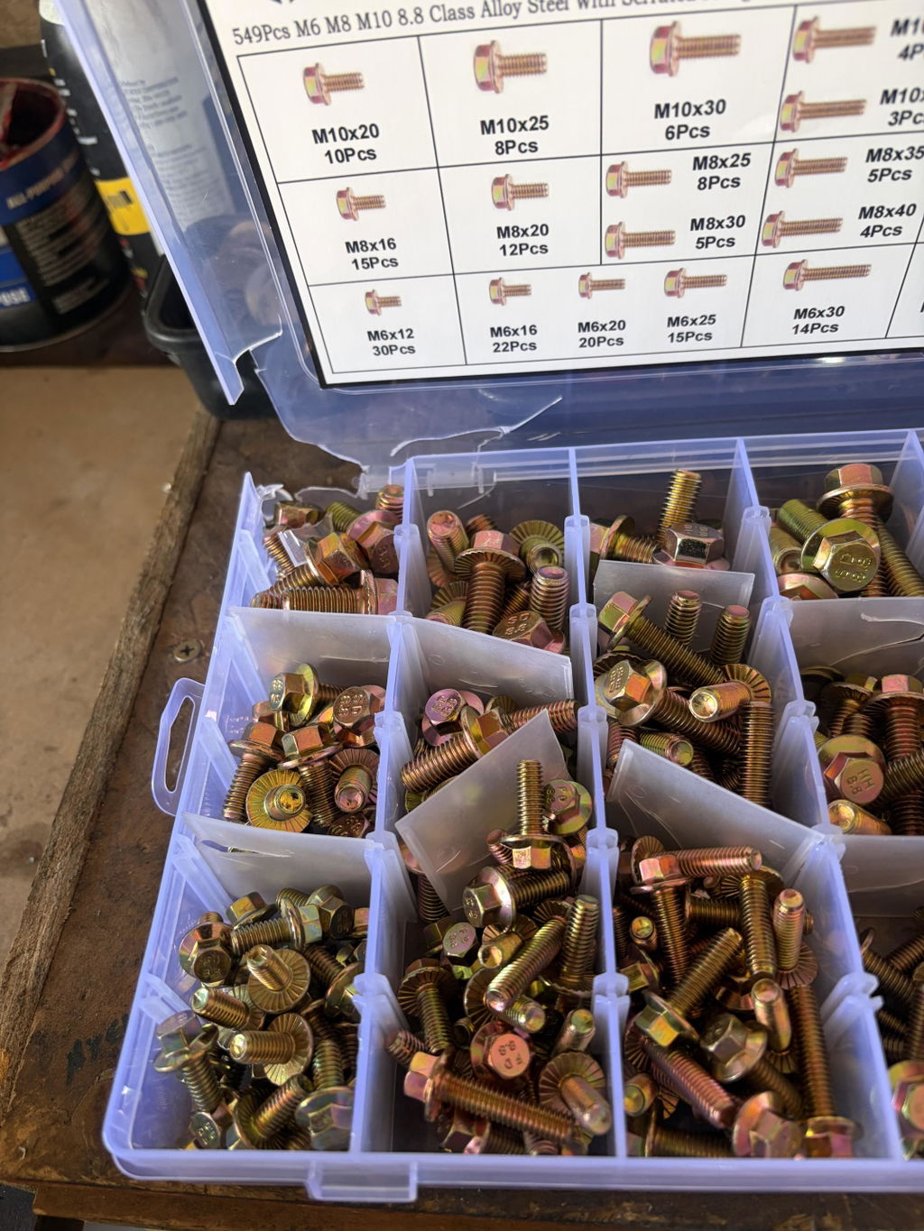
Finish on some not so good.
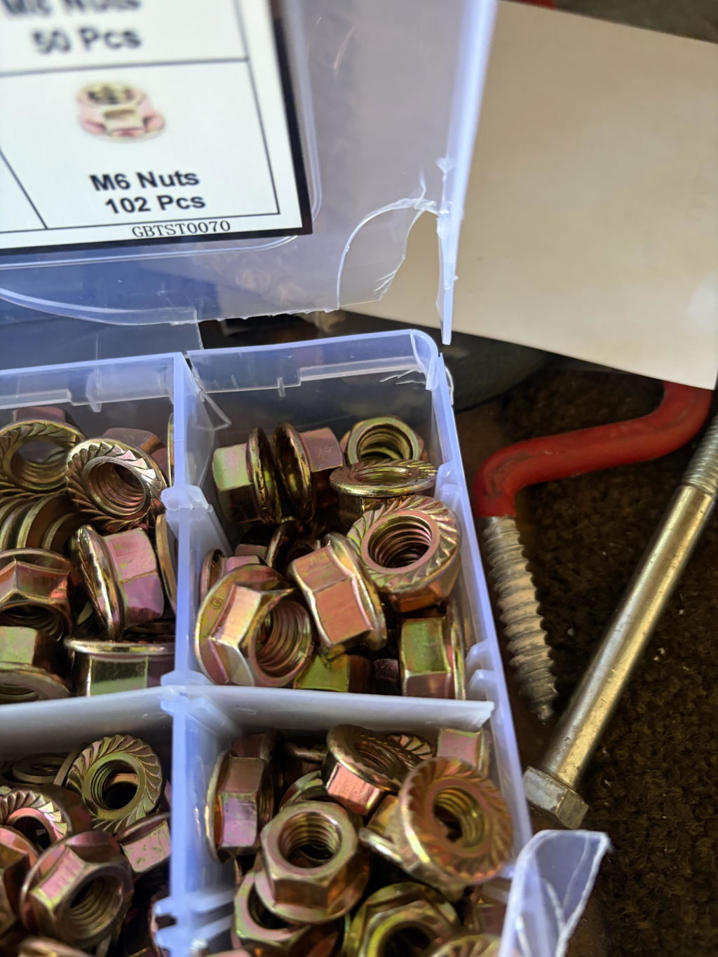
Plastic divider case arrived broken. Pretty much useless.
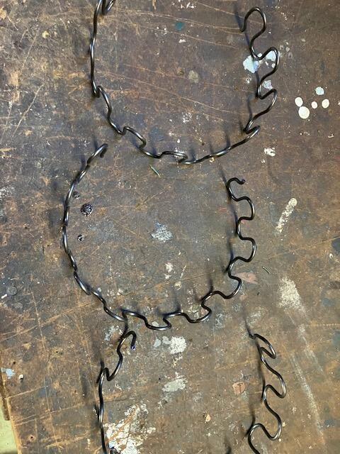
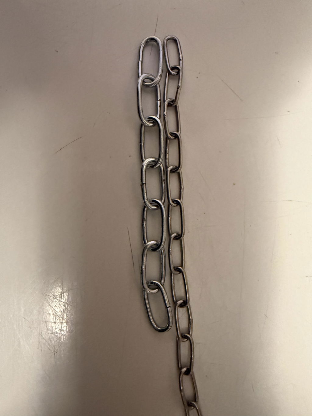
The chain is fine...but I ordered the wrong size. Nine links of the chain I ordered equals six of the size I wanted. My error...
How can I straighten out the springs? I can't use them coil uo as is.